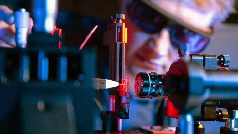
The digitalization and global interconnection have been enabled by microelectronics. For decades, the miniaturization of electronics has followed Moore's law, which predicted doubling the integration density of critical components (e.g., transistors) every 18-24 months. While this increased the computational power, the device feature size recently reached the nanoscale where quantum effects become relevant.
With classical silicon electronics, further miniaturization (and therefore increased computational power) is limited, however, quantum information processing aims to harness the same quantum effects that prevent miniaturization to gain exponential speed-ups for certain computational problems. These include factorization, searching through unstructured databases, and quantum chemistry simulations. Current leading quantum systems under investigation for quantum computing are superconducting circuits, trapped ions, solid-state defects, and photons. The latter is compatible with room temperature photonics and uses single photons as a resource. Single photon sources (SPSs) are also crucial for quantum cryptography and other quantum information applications.
Among the best state-of-the-art sources of single photons are semiconductor quantum dots, which have demonstrated simultaneous high purity and indistinguishability of emitted photons at the expense of operating at a temperature of 4 K. Single atom quantum emitters require complex ion traps and often have a low integrated single photon luminosity. Due to their simplicity, solid-state quantum emitters have recently attracted a lot of attention.
Principal investigators
Volker Deckert, University Professor Dr

Tobias Vogl, Prof. Dr
80333 München Google Maps site planExternal link